
Failure analysis is the process of collecting and analyzing data to determine the cause of a failure, often with the goal of determining corrective actions or liability. The failure analysis process relies on collecting failed components for subsequent examination of the cause or causes of failure using a wide array of methods, especially microscopy. Optical microscopy may be one of the most popular and preferred testing methods used for detecting faults, defects and problems associated with soldering and assembly. Many customers choose optical microscopy because of its speed and accuracy. Microscopy testing can verify improper construction, which can lead to stresses that can expose flaws at certain cross sections. Dino-Lite has been used increasingly for failure analysis in the microelectronics industry, especially for printed circuit boards (PCBs). Digital microscopes are practical to use and allow an efficient workflow for inspection.
Dino-Lite Digital Microscopes in PCB Failure Analysis
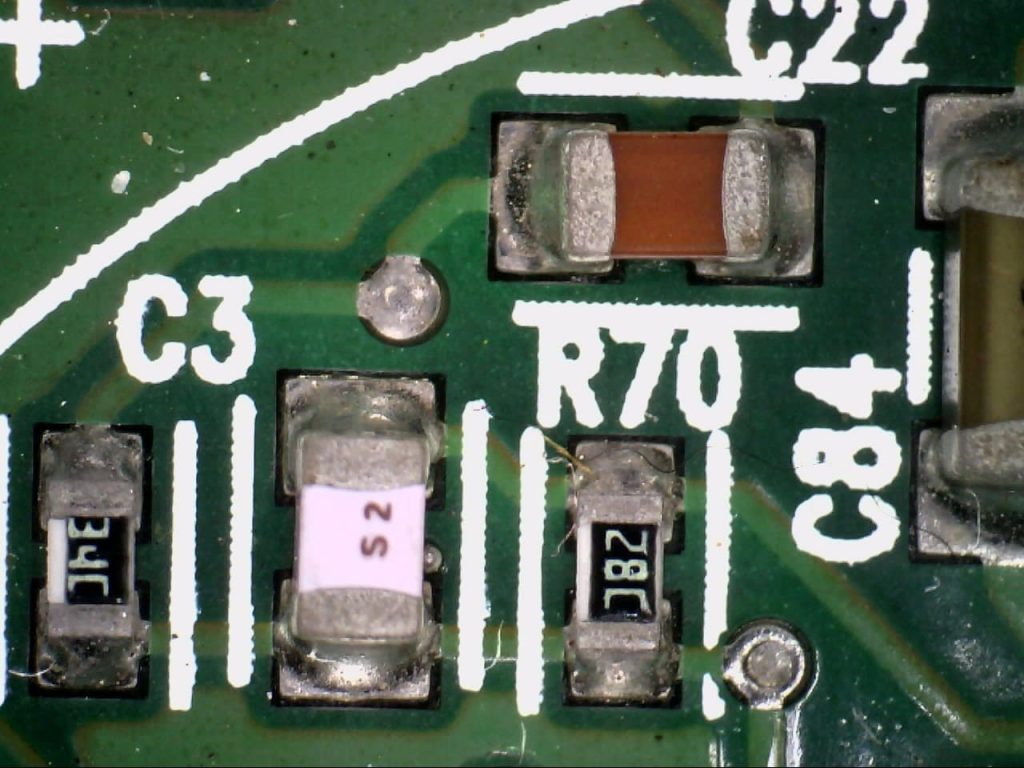
Printed circuit boards (PCBs) are the intricate lifeblood of modern electronics. When a PCB fails, malfunctions can range from minor inconveniences to complete device failure. Identifying the root cause of these failures is crucial for improving product quality and ensuring device reliability. This is where digital microscopes step in, offering a powerful tool for PCB failure analysis. Traditionally, PCB failure analysis relied on visual inspection using magnifying glasses or low-powered microscopes. While these methods provide a basic view, they often fall short when dealing with highly miniaturized components and intricate defects. Additionally, documentation of these observations can be challenging and subjective.
Dino-Lite Digital Microscopes: A High-Resolution Advantage
Dino-Lite offers a significant leap forward in PCB failure analysis. Their key advantages include:
- High Magnification: Ranging from 20x to 200x or even higher, digital microscopes allow for detailed observation of solder joints, component leads, and PCB surface features. This magnification helps identify subtle defects like cracks, voids, delamination (layer separation), and improper solder formation.
- Digital Imaging and Documentation: Captured high-resolution images and videos provide objective and sharable records of the failure site. This facilitates collaboration between engineers and failure analysts, allowing for more efficient troubleshooting.
- Enhanced Lighting: Adjustable LED illumination ensures optimal lighting for examining different areas of the PCB. Specific lighting modes can further reveal details, such as the presence of contamination or corrosion.
- Measurement Capabilities: Some digital microscopes offer built-in measurement tools for precise quantification of defect size, solder joint width, or component lead diameter. This data can be crucial for pinpointing the root cause of the failure.
Failure Analysis with Digital Microscopes: A Step-by-Step Approach
The use of digital microscopes in PCB failure analysis typically follows a systematic approach:
- Initial Inspection: The PCB is visually inspected to identify potential areas of concern like burn marks, discoloration, or component damage.
- High-Resolution Examination: The Dino-Lite digital microscope is used to examine these areas in detail, capturing images and videos for documentation.
- Defect Identification: Based on the magnified view and knowledge of common PCB failure modes, the specific defect is identified (e.g., solder joint crack, component overheating).
- Measurement and Analysis: Measurements are taken of the defect size and surrounding features. This data helps determine the potential cause and severity of the failure.
- Root Cause Determination: By analyzing the findings, the root cause of the failure can be identified, such as manufacturing process issues, component selection errors, or design flaws.
The Benefits of Dino-Lite
The use of digital microscopes in PCB failure analysis offers several advantages:
- Improved Accuracy: High-resolution magnification allows for more precise identification of failure modes, leading to more effective corrective actions.
- Enhanced Collaboration: Digital documentation facilitates communication between engineers and failure analysts, accelerating the troubleshooting process.
- Data-Driven Analysis: Measurements obtained through the microscope provide valuable data for failure analysis reports and future design improvements.
- Preventive Maintenance: By identifying recurring failure modes, manufacturers can implement preventive measures to improve overall PCB quality and reliability.
In Conclusion:
Digital microscopes are transforming PCB failure analysis. Their high magnification, digital imaging capabilities, and potential for AI integration make them an indispensable tool for identifying and understanding the root causes of PCB failures. By leveraging this technology, manufacturers can ensure the reliability of their electronic products and prevent future malfunctions.
